Electro-optic modulators based on epitaxial barium titanate integrated on silicon can reach speeds up to 50 Gbit s–1.
Optical modulators are the engines of optical communications. They encode electrical signals to optical signals by varying the intensity or phase of light. Most of the modulators use materials whose refractive index changes when an electric field is applied — a linear electro-optic phenomenon known as the Pockels effect. For decades, lithium niobate (LN), with a Pockels coefficient around ~30 pm V–1, has been the preferred material for electro-optical modulators1. Reporting in Nature Materials, Stefan Abel and co-workers2 now demonstrate modulators based on barium titanate crystals (BaTiO3, or BTO) integrated with silicon photonics. The speed of the modulators reaches a data rate higher than 50 Gbit s–1. The extracted Pockels coefficient of the BTO film is around 923 pm V–1, a value that is 30 times higher than that of LN3, and significantly surpasses previous attempts3,4,5.
The Pockels effect can only exist in materials with non-centrosymmetric crystal structure (Fig. 1a) but is absent in commodity semiconductors such as silicon. Nevertheless, silicon enjoys a high index of refraction, low optical loss in the telecommunication band, and low cost for large-scale integration and manufacture, making it the material of choice of integrated photonics6. Silicon photonics leverages the microelectronics manufacturing infrastructure to provide a large-scale integrated platform of high-density, low-loss photonic circuitry, enabling high bandwidth density and low energy consumption for both high-performance computation and data-centre interconnects6,7. Silicon, however, does not offer efficient active optical functionalities, not only in that it is prohibitive to make a silicon laser, but also for its lack of Pockels effect. Therefore, optical modulators using silicon have to utilize a ‘carrier’ effect: the injected carriers (electrons or holes) cause a shift of refractive index due to plasma dispersion8 (Fig. 1b). Because they involve the flow of electrical current as opposed to electrical field, silicon modulators are less energy efficient and operate slower than electro-optic modulators using the Pockels effect.
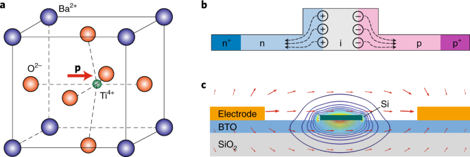
Fig. 1: BTO structure, silicon modulator and Si–BTO hybrid modulator.
a, Crystalline structure of BTO. The Ti4+ cation is displaced from the lattice centre, generating a permanent dipole moment (p) and ferroelectricity in the material. b, Scheme of a silicon waveguide modulator operating in the depletion mode. The silicon waveguide is part of a p–i–n junction. Applying a reverse bias voltage can sweep out the carriers to change silicon’s refractive index for optical modulation. c, Structure of the BTO modulator demonstrated by Abel and colleagues2. Due to the Pockels effect, the refractive index of the BTO layer underlying the silicon waveguide changes when an electric field is applied, which results in phase modulation of the guided optical mode.
It is interesting to note that LN, the most widely used Pockels material, is man-made and does not exist in nature, while its Pockels coefficient is not the highest in solid-state materials. On the other hand, BTO crystals have a Pockels coefficient of 1,640 pm V–1, more than 50 times higher than LN, while they can also be epitaxially grown as thin films on a silicon substrate. Therefore, BTO emerges as a strong candidate material for realizing Pockels electro-optic modulators integrated on silicon photonics platform.
Abel et al. first grow a single crystalline BTO film with a thin buffer layer on silicon-on-insulator (SOI) wafers by molecular beam epitaxy. This donor wafer is then flipped and bonded onto a host silicon wafer covered by silicon dioxide. Removing the silicon substrate and oxide layer of the donor wafer leaves a stack of Si/BTO/SiO2 film on the host substrate (neglecting the very thin buffer and bonding layers). Because BTO has a lower refractive index of 2.38 than silicon (3.47), photonic waveguides can be fabricated in the top silicon layer in the same way as on SOI substrates. The optical mode of the silicon waveguide couples to the underlying BTO layer — for example, with 39% power in it for the transverse-electric (TE) mode. A pair of electrodes, one on each side of the waveguide and directly on the BTO layer, are fabricated. Applying a voltage to the electrodes generates an in-plane electric field in the BTO film and induces a change in its refractive index through the Pockels effect (Fig. 1c). This results in a phase modulation to the waveguide mode. The authors make a racetrack-shaped optical resonator with electrodes placed on both straight sections. Applying a d.c. voltage of 2 V is enough to shift the resonance peak by more than a resonance linewidth, and thus can turn on and off the optical signal tuned to the resonance wavelength.
The authors, however, are cautious to quickly conclude that the observed modulation is from the Pockels effect in BTO and note that the carrier concentration change in the silicon waveguide may also be the cause. They go on to fabricate a metal–dielectric–metal plasmonic waveguide structure, in which the BTO layer is etched to a narrow fin with a width of 50 nm, and gold layers are patterned on both sides, which serve as the electrodes for the modulator as well. This plasmonic waveguide provides a high confinement of the optical field with 50% of the power in the BTO layer. Since BTO is the only dielectric in the structure, according to the paper, electro-optic modulation can only be attributed to the Pockels effect of BTO. With the plasmonic modulator, the authors demonstrate a small-signal modulation response up to 65 GHz. It is important to note that the electro-optic effect is anisotropic tensorial in crystals like BTO. Therefore, different optical modes — for example, TE and transverse-magnetic (TM) modes — with different electric field direction relative to the crystalline axis of the crystal will experience different Pockels coefficients. By mapping out this anisotropy, the authors carefully extract the largest relevant Pockels coefficient tensor element in their devices to be r42 = 923 pm V–1. This value is significantly larger than that of previously reported BTO thin film4, probably due to the high quality of the film.
It is noteworthy that there has also been significant parallel progress in integrated electro-optic modulators using conventional Pockels materials such as LN, lead zirconate titanate (PZT)9 and aluminium nitride8. The endless push on LN by the community has led to the maturity of bonded LN films on silicon substrates, which are now marketed by companies such as NanoLN (http://www.nanoln.com) on four-inch substrates as a foundry service. Loncar and co-workers10recently reported LN modulators operating up to a data rate of 210 Gbit s–1, with a low driving voltage and an energy cost less than 1 fJ bit–1. So it seems the pursuit of even better performing optical modulators using Pockels materials will continue, because they are desperately needed for energy-efficient, high-speed optical communication. With a large Pockels coefficient and the readiness to grow high-quality thin films on large silicon wafers, BTO seems to have a unique edge.