06.02.2007
РОССИЙСКАЯ АКАДЕМИЯ НАУК

УРАЛЬСКОЕ ОТДЕЛЕНИЕ

ИНСТИТУТ ХИМИИ TBEPДОГО ТЕЛА
   
| | | | |
| | | | | |
 06.02.2007   Карта сайта     Language По-русски По-английски
Новые материалы
Экология
Электротехника и обработка материалов
Медицина
Статистика публикаций


06.02.2007


Hafnium oxide helps make chips smaller and faster


05 February 2007


Intel and IBM have announced that they will use dramatically different materials to build smaller, faster transistors for their next generation of chips. 


Traditionally fashioned out of silicon, transistors are simple on/off switches that process the ones and zeros of digital electronic data. The faster its transistors switch (known as the clock speed) the more efficient the chip. Making them smaller, cheaper, faster and more energy-efficient has helped the industry to stick to Intel's co-founder Gordon Moore prediction that the number of transistors on a chip would double roughly every two years.


Microprocessors now consist of millions of transistors connected together by specific patterns of copper wires. But using current silicon technology, there are limits to the continued fulfilment of 'Moore's Law'.


In transistors, current flows between two terminals, called 'source' and 'drain'. This current is controlled by the voltage at a third terminal, the 'gate' (see diagram). For a transistor to switch efficiently, the gate needs to be isolated from source and drain by a thin piece of insulating silica, known as the dielectric. As transistors shrink, so the silica gate  insulator has thinned to just a few atomic layers. This allows quantum tunnelling of electrons, leading to current leakage across the dielectric, producing a lot of heat and poor chip performance. 


Intel transistor


The hafnium oxide insulator and metal gate have helped Intel to shrink their chips even further


© Intel


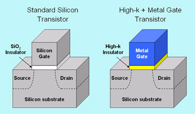
So chip manufacturers have been trying to replace the insulator with a material that has a much higher dielectric constant (high k) than silica: hafnium oxide, which has a poor ability to transmit an electric field and cuts down on electron leakage.


'Researchers have learnt to deposit very thin films of hafnium oxide and mix it with silica or silicon nitride at the molecular scale to tailor their insulating and charge storage properties,' explained Paul McIntyre from the Stanford University Engineering and Science Institute, California.


But depositing conducting silicon gate materials on top of the insulating hafnium oxide is problematic. Though hafnium oxide is tough stuff, the high temperatures needed to lay down the silicon gate damage the insulator's surface, drastically reducing the transistor's clock speed compared to typical silicon gate/silica insulator devices. Enter Intel and IBM's secret new gate materials, which can be stuck to the dielectric at less extreme conditions.


Intel chip


Close-up of a 300mm silicon test wafer made using Intel's 45nm process technology


© Intel


'Research groups worldwide have demonstrated hafnium oxide-containing transistors with a variety of gate metal materials,' explained McIntyre. 'These include titanium and hafnium nitrides, tungsten, ruthenium and ruthenium oxide and certain metal silicides,' he said.


'But mass producing reliable chips is a whole different ball game from single-device manufacture in the lab,' McIntyre told Chemistry World. 'Until we can buy the new chips and cut them open, we can't really know what gate metals Intel have chosen.' 


According to Gordon Moore, 'the implementation of high-k and metal materials marks the biggest change in transistor technology since the introduction of polysilicon gate MOS transistors in the late 1960s.'


The technology is dubbed 45 nanometre, which refers to the size of features on each chip (specifically, it is half the distance between each memory cell capable of holding one bit of information). It replaces current 65 nanometre devices, which became Intel's dominant chip technology less than a year ago. Two million of the new 45 nm transistors would cover a full stop, and with a clock speed of around 300 billion cycles per second each tick is completed in the time it takes light to travel one millimetre. McIntyre isn't alone in wanting to get his hands on the new chips, and Intel promise that production will begin in earnest later this year.


Lionel Milgrom


Дизайн и программирование N-Studio 
А Б В Г Д Е Ё Ж З И Й К Л М Н О П Р С Т У Ф Х Ц Ч Ш Щ Ъ Ы Ь Э Ю Я
  • Chen Wev   honorary member of ISSC science council

  • Harton Vladislav Vadim  honorary member of ISSC science council

  • Lichtenstain Alexandr Iosif  honorary member of ISSC science council

  • Novikov Dimirtii Leonid  honorary member of ISSC science council

  • Yakushev Mikhail Vasilii  honorary member of ISSC science council

  • © 2004-2024 ИХТТ УрО РАН
    беременность, мода, красота, здоровье, диеты, женский журнал, здоровье детей, здоровье ребенка, красота и здоровье, жизнь и здоровье, секреты красоты, воспитание ребенка рождение ребенка,пол ребенка,воспитание ребенка,ребенок дошкольного возраста, дети дошкольного возраста,грудной ребенок,обучение ребенка,родить ребенка,загадки для детей,здоровье ребенка,зачатие ребенка,второй ребенок,определение пола ребенка,будущий ребенок медицина, клиники и больницы, болезни, врач, лечение, доктор, наркология, спид, вич, алкоголизм православные знакомства, православный сайт творчeства, православные рассказы, плохие мысли, православные психологи рождение ребенка,пол ребенка,воспитание ребенка,ребенок дошкольного возраста, дети дошкольного возраста,грудной ребенок,обучение ребенка,родить ребенка,загадки для детей,здоровье ребенка,зачатие ребенка,второй ребенок,определение пола ребенка,будущий ребенок